Exclusive look inside Foxconn: FOX6 News shows you the model for the Wisconsin project
OSAKA, Japan -- As the streets of Osaka, Japan came to life on a Monday morning in December, millions of people were on the move. More than 4,000 of them would make their way to a cutting-edge industrial complex in the suburb of Sakai.
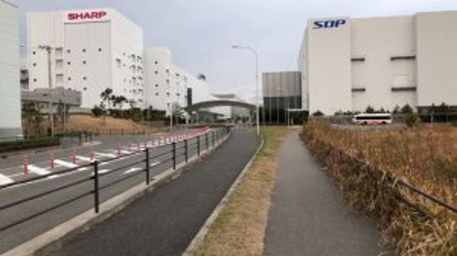
Foxconn plants near Osaka, Japan
While the signs say Sharp and SDP, which stands for Sakai Display Products, Foxconn is the majority shareholder of Sharp, and Foxconn founder Terry Gou controls SDP. It's the blueprint upon which the Wisconsin project will be built.
“We are putting the same concept design in Wisconsin,” explained SDP President Yueh Way Sun.
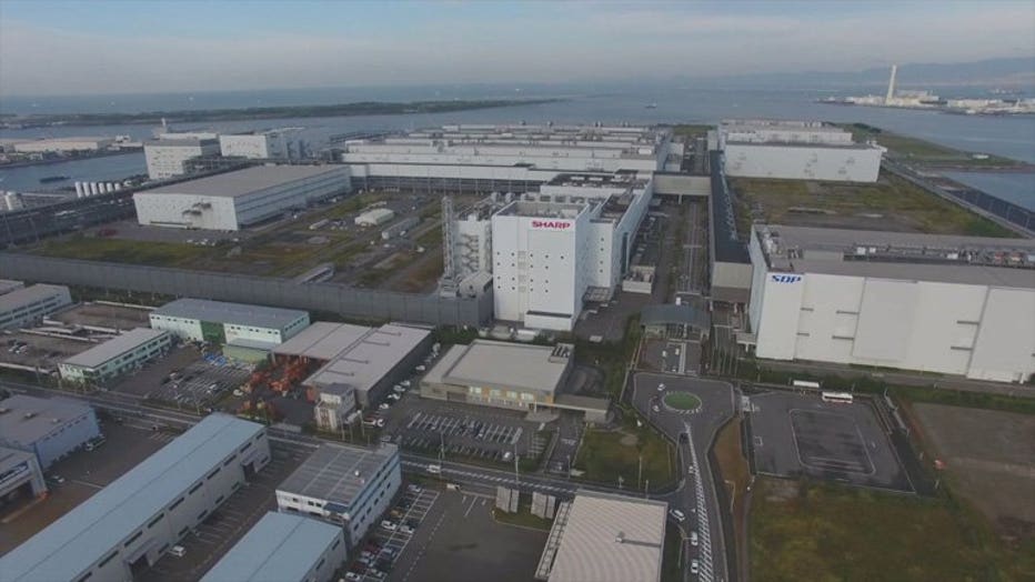
Foxconn plants near Osaka, Japan
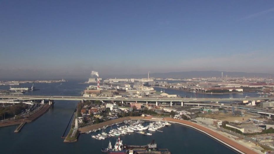
Foxconn plants near Osaka, Japan
The sprawling plant spreads across a peninsula surrounded by the blue waters of Osaka Bay. It shares the promontory with a dog park. The complex comprises a collection of vertically-integrated plants run by 17 different companies. Many oversee the on-site utilities -- the water, electrical, liquid chemical and gas production. Logistics, packaging and equipment operations take up their own area. A corning facility manufactures the mother glass. Two color filter plants create the elements that allow your eyes to see what's on the screen. And at the center of it all, the 1-point-5 million square foot LCD panel fabrication plant-- what they call the "TFT fab."
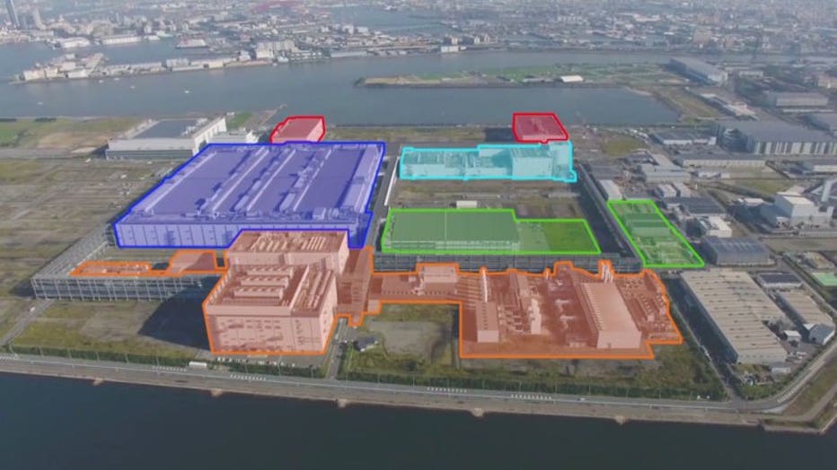
Foxconn plants near Osaka, Japan
FOX6's Brad Hicks put on a clean suit and entered part of the plant. Before you go in, you have to take a wind bath, where any last specks of dust are blown off you. The first things you notice inside the fab: the place is spotless, the machinery is massive and just about everything is automated.
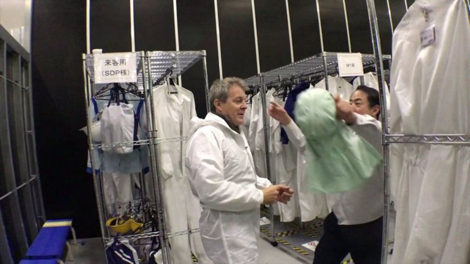
Brad Hicks dons a clean suit
It has to be. Each piece of mother glass coming in from the corning plant is the size of a small room -- more than 9 by 10 feet; and one-third the thickness of a penny. The glass goes through a series of delicate steps, much of it done in a bath of photo-safe yellow light.
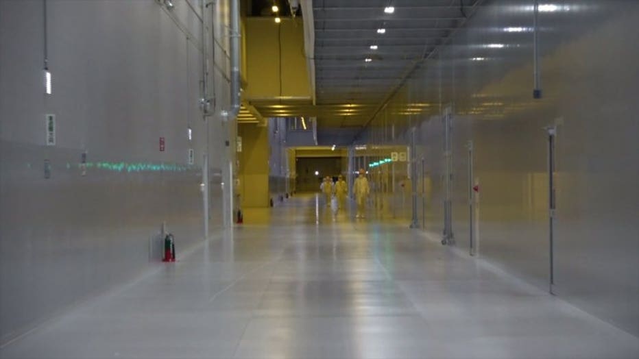
Inside the Foxconn facility

Inside the Foxconn facility
It takes 30 days and two pieces of mother glass to make an LCD panel. One is coated with special films to create transparent circuits and semiconductors-- a multi-step ballet of technology called thin film transistor processing, or TFT. That's why they call it the TFT fab. The other glass is covered with the color filters. Liquid crystals are then sandwiched between the two layers, and the laminated panels are cut into 60- and 70-inch screens -- and some, even larger.
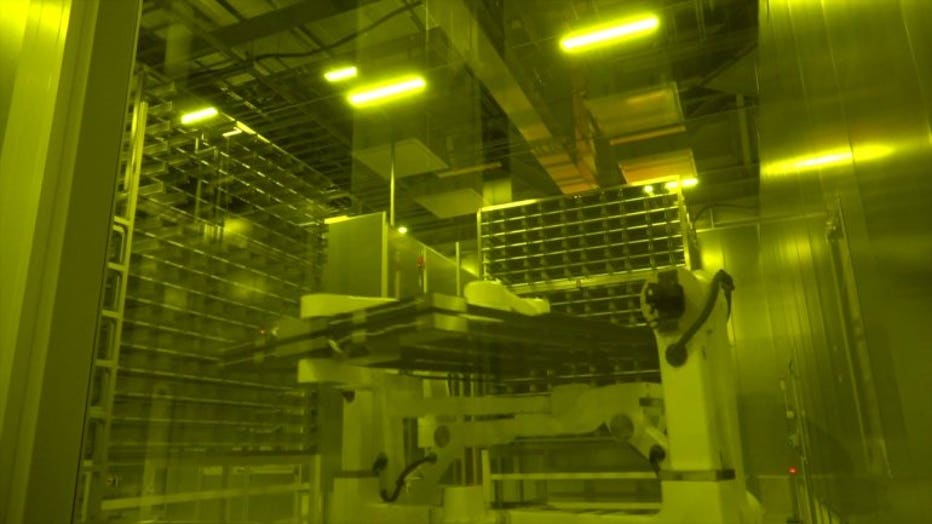
Inside the Foxconn facility
Hallways that are three football fields long overlook the fab floor.
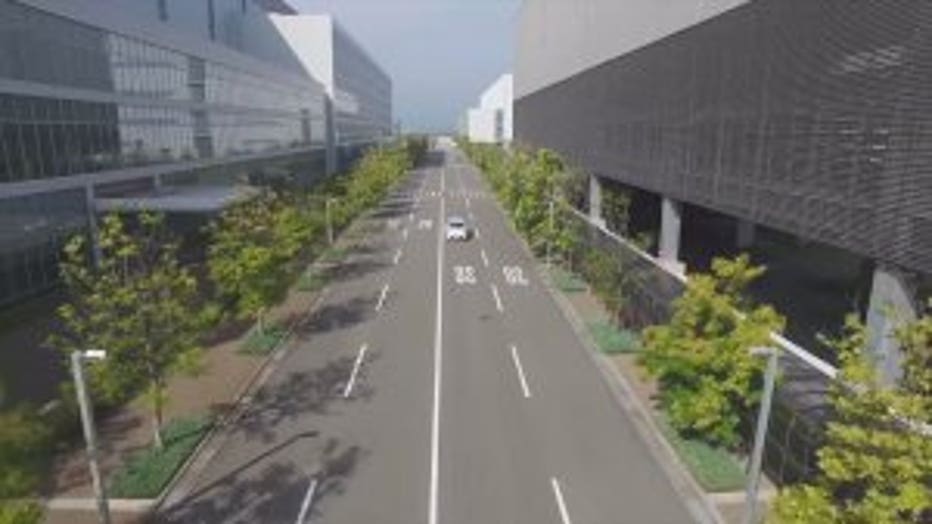
Outside the Foxconn facility
Outside, more than a mile of enclosed tramways connect the contributing plants into a seamlessly-integrated industrial machine, so you don’t see any trucks driving around. However, Yueh Way Sun said because of the cold in Wisconsin, they may put those trams underground.
“In Wisconsin, we know the cold winter, maybe drop below zero, and so we might consider underground in Wisconsin just for the weather consideration," Sun said.
The weather and where the interbuilding tram will be built is one thing, but the real difference reveals a whole new dimension. The manufacturing described above covers what’s called the front end -- the steps that create a liquid crystal display panel. But there's an entire other half to the process - the back end -- which turns that display into a usable product.
PHOTO GALLERY
The panels from Sakai are shipped off to existing plants in China for that part. Mount Pleasant will have it all.
“First, attach the driver integrated circuits,” explained Sun. “Second, attach the frames that hold the product. Third, the backlights. After we complete that, we’ll continue for the system integration and finally become the finished product available for the market. So Wisconsin has entire process, from raw material all the way down to system and finished product."
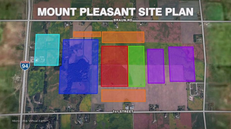
Mount Pleasant site plan for Foxconn
You can see the difference on the Mount Pleasant site plan: The areas in common with Sakai -- utilities, gas and chemicals, the corning glass plant, the color filter production, the TFT fab, and the place where the panels are cut and liquid crystals are injected. The rest (in purple) is exclusive to Racine County. While the back-end steps take up less space -- many of the jobs will be there.
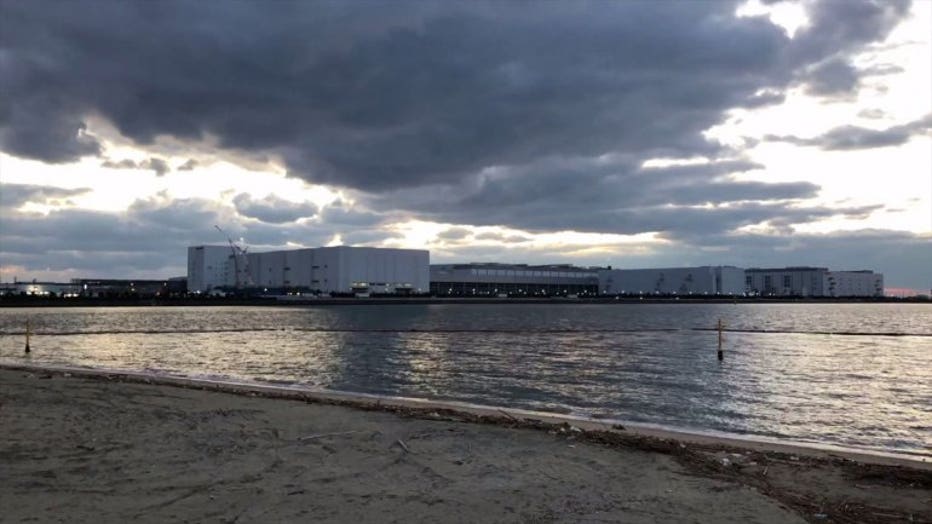
Outside the Foxconn facility
Foxconn projects the campus will be completed in 2021, but it’s going to be built in stages, and the assembly part of the process may be up and running as early as next year.
A huge first impression for Gov. Walker in the Foxconn deal
A huge first impression for Gov. Walker in the Foxconn deal
Foxconn aims to recycle 100% of the lake water is uses
Foxconn aims to recycle 100% of the lake water is uses

